INTERNATIONAL SubFAB RESEARCH LABS

INTERNATIONAL SubFAB RESEARCH LABS

Bring the Science to SubFAB. Supplement Semiconductor manufacturing technologies advancement with focused research of unwanted and harmful side effects caused by reactions of excess process materials and their byproducts. Enable and speed up development of new technologies, equipment and skills required to handle, reclaim and abate process materials




International SubFAB Research Labs (ISRL) is a privately owned company founded by semiconductor industry veterans with accumulated experience of over 80 years and professional skills spanning across diversified disciplines, such as Fab construction and operations management, hazardous materials handling and environmental regulations, process and business development.
ISRL’s vision is to fill the immense gap between industry’s desire for sustainable manufacturing and its ability to effectively address fundamental efficiency issues associated with handling, abatement and reclaim of hazardous process material waste leaving process chambers as gas emissions and liquid waste streams in FABs.
Bring the Science to SubFAB. Supplement Semiconductor manufacturing technologies advancement with focused research of unwanted and harmful side effects caused by reactions of excess process materials and their byproducts. Enable and speed up development of new technologies, equipment and skills required to handle, reclaim and abate process materials
International SubFAB Research Labs (ISRL) is a privately owned company founded by semiconductor industry veterans with accumulated experience of over 80 years and professional skills spanning across diversified disciplines, such as Fab construction and operations management, hazardous materials handling and environmental regulations, process and business development.
ISRL’s vision is to fill the immense gap between industry’s desire for sustainable manufacturing and its ability to effectively address fundamental efficiency issues associated with handling, abatement and reclaim of hazardous process material waste leaving process chambers as gas emissions and liquid waste streams in FABs.


Chemical engineer, B.Sc
Vacuum&Abatement expert
(Intel veteran)
Construction Project Manager, PMP Semiconductor equipment install expert (Intel veteran)

Business Development, MBA
Semiconductor Operations expert
(Intel veteran, former Amdocs VP)


Chemical engineer, B.Sc
Vacuum&Abatement expert
(Intel veteran)

Construction Project Manager, PMP Semiconductor equipment install expert (Intel veteran)

Business Development, MBA
Semiconductor Operations expert
(Intel veteran, former Amdocs VP)



We plan to build and manage a dedicated facility with complete infrastructure required to operate a l fleet of 300mm process tools with versatile setup of deposition and dry etching process chambers, in high volume manufacturing-like conditions, to enable a wide range of sustainability research and development projects.
Our facility will enable OTHERS to help semiconductor operations work more sustainably with sharing of best practices leading to a fast and highly efficient deployment of sustainability improvements with a business model enabling clients to both reduce their costs and amplify sustainability benefits, faster time to market for breakthroughs, innovations and operational excellence in sustainable semiconductor manufacturing.


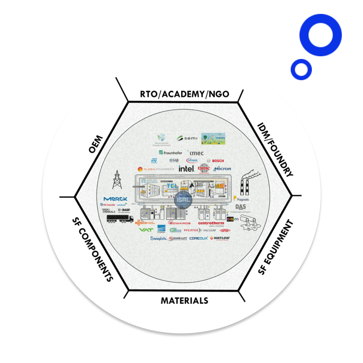
To fill an immense gap between industry’s desire for sustainable manufacturing and its ability to effectively address fundamental issues associated with handling, abatement and reclaim of hazardous process materials on their path from process chambers to air emissions and liquid waste streams generated by FABs.

© Research Labs (ISRL) 2023. All rights reserved.
עיצוב ופיתוח דיגיטל ווב Digital Web